1. Crystal Structure and Polytypism of Silicon Carbide
1.1 Cubic and Hexagonal Polytypes: From 3C to 6H and Past
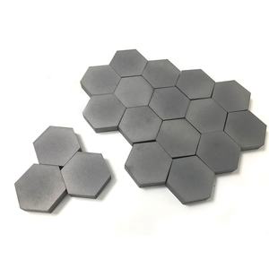
(Silicon Carbide Ceramics)
Silicon carbide (SiC) is a covalently bound ceramic made up of silicon and carbon atoms prepared in a tetrahedral control, developing one of the most intricate systems of polytypism in products scientific research.
Unlike many porcelains with a single secure crystal structure, SiC exists in over 250 recognized polytypes– distinctive stacking sequences of close-packed Si-C bilayers along the c-axis– varying from cubic 3C-SiC (likewise referred to as β-SiC) to hexagonal 6H-SiC and rhombohedral 15R-SiC.
One of the most usual polytypes used in engineering applications are 3C (cubic), 4H, and 6H (both hexagonal), each showing somewhat different electronic band frameworks and thermal conductivities.
3C-SiC, with its zinc blende framework, has the narrowest bandgap (~ 2.3 eV) and is normally grown on silicon substrates for semiconductor gadgets, while 4H-SiC uses premium electron mobility and is liked for high-power electronic devices.
The solid covalent bonding and directional nature of the Si– C bond give outstanding firmness, thermal security, and resistance to creep and chemical attack, making SiC ideal for severe environment applications.
1.2 Flaws, Doping, and Digital Feature
In spite of its structural intricacy, SiC can be doped to attain both n-type and p-type conductivity, enabling its usage in semiconductor devices.
Nitrogen and phosphorus work as contributor pollutants, presenting electrons right into the transmission band, while light weight aluminum and boron act as acceptors, producing openings in the valence band.
Nonetheless, p-type doping performance is restricted by high activation powers, specifically in 4H-SiC, which postures difficulties for bipolar device design.
Indigenous defects such as screw misplacements, micropipes, and piling mistakes can weaken device performance by functioning as recombination centers or leak courses, demanding high-quality single-crystal growth for electronic applications.
The broad bandgap (2.3– 3.3 eV depending on polytype), high breakdown electric area (~ 3 MV/cm), and superb thermal conductivity (~ 3– 4 W/m · K for 4H-SiC) make SiC far above silicon in high-temperature, high-voltage, and high-frequency power electronic devices.
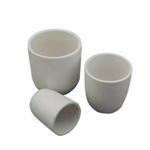
2. Processing and Microstructural Design
( Silicon Carbide Ceramics)
2.1 Sintering and Densification Methods
Silicon carbide is naturally tough to compress due to its solid covalent bonding and reduced self-diffusion coefficients, needing sophisticated processing methods to achieve full density without additives or with minimal sintering aids.
Pressureless sintering of submicron SiC powders is feasible with the addition of boron and carbon, which promote densification by getting rid of oxide layers and boosting solid-state diffusion.
Hot pressing uses uniaxial stress throughout heating, allowing full densification at lower temperatures (~ 1800– 2000 ° C )and producing fine-grained, high-strength elements ideal for reducing devices and use components.
For large or complicated forms, response bonding is utilized, where porous carbon preforms are penetrated with liquified silicon at ~ 1600 ° C, forming β-SiC in situ with very little shrinking.
Nonetheless, recurring free silicon (~ 5– 10%) continues to be in the microstructure, limiting high-temperature efficiency and oxidation resistance above 1300 ° C.
2.2 Additive Manufacturing and Near-Net-Shape Manufacture
Current advancements in additive manufacturing (AM), particularly binder jetting and stereolithography utilizing SiC powders or preceramic polymers, enable the manufacture of intricate geometries formerly unattainable with standard approaches.
In polymer-derived ceramic (PDC) paths, fluid SiC forerunners are formed by means of 3D printing and then pyrolyzed at heats to produce amorphous or nanocrystalline SiC, usually needing more densification.
These techniques decrease machining costs and product waste, making SiC more available for aerospace, nuclear, and warm exchanger applications where detailed layouts improve performance.
Post-processing actions such as chemical vapor seepage (CVI) or liquid silicon seepage (LSI) are sometimes made use of to improve density and mechanical integrity.
3. Mechanical, Thermal, and Environmental Efficiency
3.1 Strength, Hardness, and Use Resistance
Silicon carbide places amongst the hardest known products, with a Mohs solidity of ~ 9.5 and Vickers solidity exceeding 25 Grade point average, making it very resistant to abrasion, disintegration, and scratching.
Its flexural stamina typically ranges from 300 to 600 MPa, relying on handling method and grain size, and it maintains strength at temperatures as much as 1400 ° C in inert atmospheres.
Fracture toughness, while moderate (~ 3– 4 MPa · m ¹/ ²), is sufficient for numerous architectural applications, especially when integrated with fiber support in ceramic matrix composites (CMCs).
SiC-based CMCs are used in generator blades, combustor liners, and brake systems, where they offer weight financial savings, gas effectiveness, and prolonged service life over metallic counterparts.
Its outstanding wear resistance makes SiC suitable for seals, bearings, pump elements, and ballistic armor, where longevity under rough mechanical loading is critical.
3.2 Thermal Conductivity and Oxidation Stability
One of SiC’s most important homes is its high thermal conductivity– as much as 490 W/m · K for single-crystal 4H-SiC and ~ 30– 120 W/m · K for polycrystalline kinds– exceeding that of several steels and making it possible for effective heat dissipation.
This residential or commercial property is important in power electronics, where SiC gadgets generate less waste heat and can run at higher power densities than silicon-based tools.
At raised temperature levels in oxidizing atmospheres, SiC creates a protective silica (SiO TWO) layer that slows additional oxidation, giving excellent environmental durability up to ~ 1600 ° C.
Nonetheless, in water vapor-rich atmospheres, this layer can volatilize as Si(OH)₄, causing sped up degradation– a vital challenge in gas wind turbine applications.
4. Advanced Applications in Energy, Electronics, and Aerospace
4.1 Power Electronics and Semiconductor Instruments
Silicon carbide has actually revolutionized power electronics by making it possible for tools such as Schottky diodes, MOSFETs, and JFETs that operate at greater voltages, frequencies, and temperatures than silicon equivalents.
These devices reduce energy losses in electrical cars, renewable resource inverters, and commercial electric motor drives, contributing to worldwide power performance enhancements.
The capability to run at junction temperatures over 200 ° C permits simplified air conditioning systems and boosted system integrity.
Additionally, SiC wafers are made use of as substratums for gallium nitride (GaN) epitaxy in high-electron-mobility transistors (HEMTs), integrating the benefits of both wide-bandgap semiconductors.
4.2 Nuclear, Aerospace, and Optical Solutions
In atomic power plants, SiC is a crucial component of accident-tolerant fuel cladding, where its reduced neutron absorption cross-section, radiation resistance, and high-temperature stamina enhance security and efficiency.
In aerospace, SiC fiber-reinforced composites are used in jet engines and hypersonic vehicles for their lightweight and thermal stability.
Furthermore, ultra-smooth SiC mirrors are employed precede telescopes as a result of their high stiffness-to-density proportion, thermal security, and polishability to sub-nanometer roughness.
In recap, silicon carbide porcelains stand for a cornerstone of modern advanced products, combining extraordinary mechanical, thermal, and electronic buildings.
Via accurate control of polytype, microstructure, and handling, SiC continues to allow technological innovations in power, transport, and severe setting design.
5. Distributor
TRUNNANO is a supplier of Spherical Tungsten Powder with over 12 years of experience in nano-building energy conservation and nanotechnology development. It accepts payment via Credit Card, T/T, West Union and Paypal. Trunnano will ship the goods to customers overseas through FedEx, DHL, by air, or by sea. If you want to know more about Spherical Tungsten Powder, please feel free to contact us and send an inquiry(sales5@nanotrun.com).
Tags: silicon carbide ceramic,silicon carbide ceramic products, industry ceramic
All articles and pictures are from the Internet. If there are any copyright issues, please contact us in time to delete.
Inquiry us