1. Crystal Structure and Polytypism of Silicon Carbide
1.1 Cubic and Hexagonal Polytypes: From 3C to 6H and Past
(Silicon Carbide Ceramics)
Silicon carbide (SiC) is a covalently bonded ceramic made up of silicon and carbon atoms arranged in a tetrahedral coordination, creating among one of the most intricate systems of polytypism in materials science.
Unlike the majority of ceramics with a solitary steady crystal structure, SiC exists in over 250 recognized polytypes– unique piling sequences of close-packed Si-C bilayers along the c-axis– ranging from cubic 3C-SiC (additionally referred to as β-SiC) to hexagonal 6H-SiC and rhombohedral 15R-SiC.
The most typical polytypes made use of in design applications are 3C (cubic), 4H, and 6H (both hexagonal), each displaying somewhat various electronic band frameworks and thermal conductivities.
3C-SiC, with its zinc blende structure, has the narrowest bandgap (~ 2.3 eV) and is typically expanded on silicon substratums for semiconductor devices, while 4H-SiC uses exceptional electron movement and is chosen for high-power electronics.
The solid covalent bonding and directional nature of the Si– C bond confer remarkable solidity, thermal security, and resistance to slip and chemical strike, making SiC ideal for severe setting applications.
1.2 Issues, Doping, and Electronic Feature
In spite of its structural intricacy, SiC can be doped to attain both n-type and p-type conductivity, enabling its use in semiconductor devices.
Nitrogen and phosphorus act as benefactor pollutants, presenting electrons right into the conduction band, while aluminum and boron serve as acceptors, creating holes in the valence band.
Nonetheless, p-type doping efficiency is limited by high activation powers, particularly in 4H-SiC, which positions difficulties for bipolar tool design.
Indigenous defects such as screw misplacements, micropipes, and piling faults can weaken device efficiency by functioning as recombination centers or leakage paths, demanding top notch single-crystal development for digital applications.
The large bandgap (2.3– 3.3 eV relying on polytype), high break down electric area (~ 3 MV/cm), and excellent thermal conductivity (~ 3– 4 W/m · K for 4H-SiC) make SiC much above silicon in high-temperature, high-voltage, and high-frequency power electronics.
2. Processing and Microstructural Design
( Silicon Carbide Ceramics)
2.1 Sintering and Densification Techniques
Silicon carbide is naturally hard to densify because of its solid covalent bonding and low self-diffusion coefficients, needing advanced handling methods to accomplish complete density without ingredients or with very little sintering aids.
Pressureless sintering of submicron SiC powders is possible with the enhancement of boron and carbon, which advertise densification by removing oxide layers and enhancing solid-state diffusion.
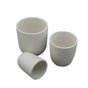
Warm pressing uses uniaxial stress during heating, making it possible for complete densification at reduced temperature levels (~ 1800– 2000 ° C )and generating fine-grained, high-strength elements suitable for cutting tools and put on components.
For large or complicated forms, response bonding is used, where porous carbon preforms are infiltrated with molten silicon at ~ 1600 ° C, creating β-SiC in situ with minimal shrinking.
However, residual totally free silicon (~ 5– 10%) stays in the microstructure, limiting high-temperature efficiency and oxidation resistance over 1300 ° C.
2.2 Additive Manufacturing and Near-Net-Shape Manufacture
Current breakthroughs in additive manufacturing (AM), especially binder jetting and stereolithography utilizing SiC powders or preceramic polymers, enable the construction of complex geometries previously unattainable with conventional techniques.
In polymer-derived ceramic (PDC) paths, fluid SiC forerunners are formed using 3D printing and after that pyrolyzed at high temperatures to yield amorphous or nanocrystalline SiC, often requiring more densification.
These strategies minimize machining prices and product waste, making SiC extra easily accessible for aerospace, nuclear, and heat exchanger applications where complex designs improve efficiency.
Post-processing actions such as chemical vapor infiltration (CVI) or liquid silicon seepage (LSI) are occasionally made use of to boost density and mechanical stability.
3. Mechanical, Thermal, and Environmental Efficiency
3.1 Toughness, Firmness, and Use Resistance
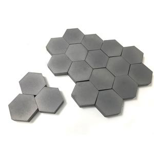
Silicon carbide ranks amongst the hardest recognized materials, with a Mohs solidity of ~ 9.5 and Vickers firmness going beyond 25 GPa, making it very resistant to abrasion, disintegration, and scraping.
Its flexural strength generally ranges from 300 to 600 MPa, relying on handling method and grain dimension, and it maintains stamina at temperature levels approximately 1400 ° C in inert ambiences.
Fracture sturdiness, while moderate (~ 3– 4 MPa · m ONE/ TWO), suffices for many architectural applications, particularly when incorporated with fiber support in ceramic matrix compounds (CMCs).
SiC-based CMCs are utilized in wind turbine blades, combustor linings, and brake systems, where they use weight financial savings, gas efficiency, and expanded service life over metallic counterparts.
Its excellent wear resistance makes SiC suitable for seals, bearings, pump components, and ballistic armor, where sturdiness under harsh mechanical loading is vital.
3.2 Thermal Conductivity and Oxidation Security
Among SiC’s most important residential or commercial properties is its high thermal conductivity– approximately 490 W/m · K for single-crystal 4H-SiC and ~ 30– 120 W/m · K for polycrystalline kinds– surpassing that of lots of metals and enabling reliable warm dissipation.
This residential or commercial property is essential in power electronics, where SiC gadgets generate less waste warm and can operate at higher power thickness than silicon-based tools.
At elevated temperatures in oxidizing atmospheres, SiC creates a safety silica (SiO TWO) layer that slows down more oxidation, providing good ecological resilience as much as ~ 1600 ° C.
Nevertheless, in water vapor-rich environments, this layer can volatilize as Si(OH)₄, leading to accelerated degradation– a key obstacle in gas turbine applications.
4. Advanced Applications in Energy, Electronics, and Aerospace
4.1 Power Electronic Devices and Semiconductor Instruments
Silicon carbide has revolutionized power electronics by enabling devices such as Schottky diodes, MOSFETs, and JFETs that operate at higher voltages, regularities, and temperature levels than silicon matchings.
These gadgets reduce energy losses in electrical lorries, renewable resource inverters, and industrial motor drives, contributing to worldwide energy effectiveness improvements.
The capability to operate at junction temperatures over 200 ° C allows for streamlined cooling systems and raised system reliability.
In addition, SiC wafers are used as substrates for gallium nitride (GaN) epitaxy in high-electron-mobility transistors (HEMTs), incorporating the benefits of both wide-bandgap semiconductors.
4.2 Nuclear, Aerospace, and Optical Solutions
In nuclear reactors, SiC is a vital part of accident-tolerant fuel cladding, where its reduced neutron absorption cross-section, radiation resistance, and high-temperature strength improve safety and security and efficiency.
In aerospace, SiC fiber-reinforced compounds are made use of in jet engines and hypersonic automobiles for their lightweight and thermal stability.
Additionally, ultra-smooth SiC mirrors are employed in space telescopes due to their high stiffness-to-density ratio, thermal stability, and polishability to sub-nanometer roughness.
In summary, silicon carbide ceramics stand for a cornerstone of contemporary sophisticated products, combining remarkable mechanical, thermal, and digital homes.
Through precise control of polytype, microstructure, and processing, SiC remains to make it possible for technical developments in energy, transport, and severe atmosphere design.
5. Provider
TRUNNANO is a supplier of Spherical Tungsten Powder with over 12 years of experience in nano-building energy conservation and nanotechnology development. It accepts payment via Credit Card, T/T, West Union and Paypal. Trunnano will ship the goods to customers overseas through FedEx, DHL, by air, or by sea. If you want to know more about Spherical Tungsten Powder, please feel free to contact us and send an inquiry(sales5@nanotrun.com).
Tags: silicon carbide ceramic,silicon carbide ceramic products, industry ceramic
All articles and pictures are from the Internet. If there are any copyright issues, please contact us in time to delete.
Inquiry us