1. Crystal Framework and Split Anisotropy
1.1 The 2H and 1T Polymorphs: Architectural and Digital Duality
(Molybdenum Disulfide)
Molybdenum disulfide (MoS ₂) is a split transition steel dichalcogenide (TMD) with a chemical formula including one molybdenum atom sandwiched in between 2 sulfur atoms in a trigonal prismatic sychronisation, creating covalently bound S– Mo– S sheets.
These specific monolayers are stacked vertically and held together by weak van der Waals pressures, making it possible for easy interlayer shear and exfoliation down to atomically slim two-dimensional (2D) crystals– an architectural feature central to its varied useful roles.
MoS two exists in multiple polymorphic kinds, one of the most thermodynamically stable being the semiconducting 2H phase (hexagonal proportion), where each layer displays a straight bandgap of ~ 1.8 eV in monolayer form that transitions to an indirect bandgap (~ 1.3 eV) in bulk, a phenomenon vital for optoelectronic applications.
On the other hand, the metastable 1T phase (tetragonal symmetry) adopts an octahedral sychronisation and acts as a metallic conductor because of electron donation from the sulfur atoms, enabling applications in electrocatalysis and conductive composites.
Phase changes in between 2H and 1T can be generated chemically, electrochemically, or with pressure engineering, offering a tunable platform for developing multifunctional devices.
The capacity to maintain and pattern these stages spatially within a single flake opens pathways for in-plane heterostructures with distinct electronic domain names.
1.2 Problems, Doping, and Side States
The performance of MoS ₂ in catalytic and digital applications is highly conscious atomic-scale flaws and dopants.
Intrinsic factor issues such as sulfur openings act as electron donors, raising n-type conductivity and functioning as energetic sites for hydrogen advancement reactions (HER) in water splitting.
Grain limits and line flaws can either hamper fee transport or develop local conductive pathways, depending upon their atomic setup.
Regulated doping with transition steels (e.g., Re, Nb) or chalcogens (e.g., Se) enables fine-tuning of the band structure, provider concentration, and spin-orbit combining impacts.
Especially, the sides of MoS ₂ nanosheets, especially the metallic Mo-terminated (10– 10) sides, exhibit considerably greater catalytic activity than the inert basic plane, motivating the design of nanostructured stimulants with taken full advantage of side exposure.
( Molybdenum Disulfide)
These defect-engineered systems exemplify just how atomic-level adjustment can transform a normally taking place mineral right into a high-performance useful product.
2. Synthesis and Nanofabrication Methods
2.1 Bulk and Thin-Film Production Approaches
Natural molybdenite, the mineral form of MoS TWO, has been utilized for decades as a strong lubricating substance, but contemporary applications require high-purity, structurally regulated artificial types.
Chemical vapor deposition (CVD) is the dominant approach for producing large-area, high-crystallinity monolayer and few-layer MoS ₂ films on substratums such as SiO ₂/ Si, sapphire, or versatile polymers.
In CVD, molybdenum and sulfur forerunners (e.g., MoO four and S powder) are vaporized at high temperatures (700– 1000 ° C )in control environments, enabling layer-by-layer development with tunable domain size and alignment.
Mechanical exfoliation (“scotch tape method”) continues to be a criteria for research-grade samples, producing ultra-clean monolayers with very little issues, though it does not have scalability.
Liquid-phase exfoliation, including sonication or shear mixing of mass crystals in solvents or surfactant services, generates colloidal dispersions of few-layer nanosheets appropriate for finishes, compounds, and ink formulations.
2.2 Heterostructure Integration and Gadget Patterning
Real potential of MoS two emerges when incorporated right into vertical or side heterostructures with other 2D products such as graphene, hexagonal boron nitride (h-BN), or WSe ₂.
These van der Waals heterostructures make it possible for the layout of atomically specific gadgets, including tunneling transistors, photodetectors, and light-emitting diodes (LEDs), where interlayer cost and energy transfer can be engineered.
Lithographic pattern and etching methods allow the construction of nanoribbons, quantum dots, and field-effect transistors (FETs) with channel sizes to tens of nanometers.
Dielectric encapsulation with h-BN protects MoS ₂ from ecological deterioration and minimizes fee spreading, considerably enhancing provider flexibility and device security.
These construction developments are crucial for transitioning MoS two from lab interest to viable part in next-generation nanoelectronics.
3. Practical Features and Physical Mechanisms
3.1 Tribological Habits and Solid Lubrication
Among the oldest and most enduring applications of MoS ₂ is as a completely dry strong lube in severe environments where fluid oils stop working– such as vacuum, high temperatures, or cryogenic problems.
The low interlayer shear stamina of the van der Waals void permits very easy gliding between S– Mo– S layers, causing a coefficient of friction as reduced as 0.03– 0.06 under ideal problems.
Its performance is even more enhanced by strong adhesion to steel surfaces and resistance to oxidation approximately ~ 350 ° C in air, past which MoO six development enhances wear.
MoS ₂ is extensively used in aerospace mechanisms, air pump, and weapon elements, frequently used as a coating using burnishing, sputtering, or composite unification right into polymer matrices.
Current research studies reveal that moisture can deteriorate lubricity by increasing interlayer attachment, motivating research right into hydrophobic coverings or crossbreed lubricants for enhanced environmental security.
3.2 Digital and Optoelectronic Reaction
As a direct-gap semiconductor in monolayer kind, MoS ₂ exhibits strong light-matter communication, with absorption coefficients surpassing 10 ⁵ cm ⁻¹ and high quantum return in photoluminescence.
This makes it perfect for ultrathin photodetectors with fast feedback times and broadband sensitivity, from noticeable to near-infrared wavelengths.
Field-effect transistors based upon monolayer MoS ₂ show on/off ratios > 10 eight and provider movements as much as 500 centimeters TWO/ V · s in put on hold samples, though substrate communications generally limit functional worths to 1– 20 centimeters TWO/ V · s.
Spin-valley combining, an effect of strong spin-orbit interaction and busted inversion symmetry, allows valleytronics– an unique paradigm for information inscribing using the valley level of flexibility in energy space.
These quantum phenomena setting MoS two as a prospect for low-power reasoning, memory, and quantum computer elements.
4. Applications in Energy, Catalysis, and Arising Technologies
4.1 Electrocatalysis for Hydrogen Advancement Response (HER)
MoS two has actually emerged as a promising non-precious choice to platinum in the hydrogen development response (HER), a crucial process in water electrolysis for environment-friendly hydrogen manufacturing.
While the basal aircraft is catalytically inert, side websites and sulfur jobs display near-optimal hydrogen adsorption cost-free energy (ΔG_H * ≈ 0), similar to Pt.
Nanostructuring methods– such as producing vertically straightened nanosheets, defect-rich films, or doped crossbreeds with Ni or Carbon monoxide– make the most of energetic website density and electric conductivity.
When incorporated right into electrodes with conductive sustains like carbon nanotubes or graphene, MoS two attains high current densities and long-lasting security under acidic or neutral problems.
Additional enhancement is attained by supporting the metallic 1T phase, which improves inherent conductivity and reveals extra active sites.
4.2 Versatile Electronics, Sensors, and Quantum Gadgets
The mechanical flexibility, transparency, and high surface-to-volume proportion of MoS two make it excellent for adaptable and wearable electronic devices.
Transistors, reasoning circuits, and memory devices have actually been shown on plastic substrates, enabling flexible displays, health monitors, and IoT sensing units.
MoS ₂-based gas sensing units show high level of sensitivity to NO TWO, NH SIX, and H ₂ O because of bill transfer upon molecular adsorption, with reaction times in the sub-second array.
In quantum innovations, MoS ₂ hosts localized excitons and trions at cryogenic temperatures, and strain-induced pseudomagnetic fields can trap providers, allowing single-photon emitters and quantum dots.
These advancements highlight MoS two not just as a practical material yet as a system for discovering fundamental physics in minimized measurements.
In recap, molybdenum disulfide exhibits the merging of timeless materials science and quantum engineering.
From its ancient function as a lube to its contemporary release in atomically thin electronic devices and energy systems, MoS two continues to redefine the boundaries of what is possible in nanoscale products style.
As synthesis, characterization, and integration techniques development, its impact across science and technology is poised to increase also better.
5. Provider
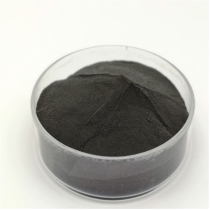
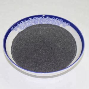
TRUNNANO is a globally recognized Molybdenum Disulfide manufacturer and supplier of compounds with more than 12 years of expertise in the highest quality nanomaterials and other chemicals. The company develops a variety of powder materials and chemicals. Provide OEM service. If you need high quality Molybdenum Disulfide, please feel free to contact us. You can click on the product to contact us.
Tags: Molybdenum Disulfide, nano molybdenum disulfide, MoS2
All articles and pictures are from the Internet. If there are any copyright issues, please contact us in time to delete.
Inquiry us